martes, 29 de enero de 2013

IPC/WHMA-A-620B

Requirements and Acceptance for Cable and Wire Harness Assemblies


NEW! Includes greatly expanded criteria for molding, potting, splicing, crimp contacts without insulation support, inline insulation displacement connectors, connectorization, rigid and conformable cable, flexible sleeving, broomstitching, testing, and more.


Revision B remains the only industry-consensus standard for Requirements and Acceptance of Cable and Wire Harness Assemblies. IPC and the Wire Harness Manufacturers Association (WHMA) have continued to work together to develop this significant update.


This revision now has 682 full-color pictures and illustrations – 125 are new or updated. Included in the 19 chapters are criteria for wire prep, soldering to terminals, crimping of stamped and formed contacts and machined contacts, insulation displacement connectors, ultrasonic welding, splicing, connectors, molding, marking, coax/biax cables, wrapping/lacing, shielding, assembly and wire-wrap terminations. 400 pages. Released October 2012.


The training and certification programs for Revision B are in development and targeted for release in April 2013. Contact joselmartinez@owen-gl.com .

FLUXES.

En este ariculo hablaremos un poco sobre los tipos de flux y sus caracteristicas principales.

Flux es un químico que ayuda a expandir el mojado en los metales removiendo ligeramente la oxidación y  protege la superficie de la re-oxidación durante la operación de soldadura.

 ¿Cómo funciona el flux?

El flux refluye antes que la soldadura, limpiando y ayudando a activar el proceso de calentamiento. La oxidación se forma en todos los metales expuestos al aire.
El flux retira ligeramente la oxidacion de la superficies con las que esta en contacto. Expande el mojado de la soldadura en la base metalica de la superficie.

Fluxes compatibles con la soldadura libre de plomo

Están disponibles en una variedad de químicos y envases.
Disponibles en compuestos libres de volátiles orgánicos (VOC) y químicas en base a alcohol para residuos ultra bajos.
Para una soldadura convencional exitosa, la selección del flux apropiado es tan importante como la elección del estaño y los componentes de la maquinaria.
El flux debe eliminar el óxido, la capa externa y deslustre de la superficie, para conseguir una placa limpia que permita un mojado y soldadura óptimos.

ACCIÓN DEL FLUX


El flux refluye a una temperatura mas baja que la soldadura.  Mueve la soldadura derretida para limpiar la oxidación de la conexión.
Flux extra debe ser evitado en lo posible en soldadura manual, ya que los residuos de fluxes utilizados en soldadura lead free normalmente serán más activos y sus residuos más dañinos para el tablero.
El uso de extractores de humo pueden ser requeridos cuando se usen fluxes libres de plomo. Consulta el MSDS para más informacion.
 

PROPOSITO DEL FLUX


El principal propósito de flux es eliminar los óxidos y penetrar en las capas, evitar la oxidación durante el calentamiento y la reducción de fricción/tensión superficial. Además, el flux debe ser térmicamente estable, fácil de ser desplazado por la soldadura fundida, no perjudicial para los componentes, y de sencilla eliminación.

Un material, fluirá libremente sobre una superficie, sólo si, al hacerlo, el total de la energía libre del sistema es reducido. En el caso de la soldadura, la energía de una superficie limpia es mucho mayor que una superficie sucia, por lo tanto, será más probable un buen flujo de soldadura.

Los principales efectos de un flux son los siguientes:


Químicamente: Reduce los óxidos de la superficie a soldar y protege la superficie (recubriéndola) de la re-oxidación.
Térmicamente: Asiste en la transferencia de calor, de la fuente de calor con el componente que será soldado (especialmente crítico para soldadura manual).
Físicamente: Transporta los óxidos y otros componentes reactivos fuera de la zona que está siendo soldada.
Generalmente los fluxes son diferenciados por el grado de agresividad, refiriéndose a la actividad del flux. Cuanto mayor sea el grado de actividad, el flux será más peligroso y sus residuos afectan a la confiabilidad del ensamble  que se esté trabajando. Por esta razón, las normas militares permiten flux tipo R o RMA, pero prohibieron el uso de los fluxes de mayor actividad, como la RA. El potencial de corrosión y posterior fracaso del circuito se considera demasiado importante como para permitirse en aplicaciones de alta confiabilidad.
 Fluxes "no clean" pueden dejar residuos en el ensamble, ya que sus resiudos son benignos (a corto, mediano y largo)  siempre y cuando sean activados termicamente de forma adecuada, ya que su proposito es no tener que limpiar residios, no obstante,  unicamente estas seguro de estos parametros mientras no se utilice una cantidad de flux extra a la que trae el nucleo de la soldadura de alambre o la soldadura en pasta.  Es importante considerar que cuando el flux es "clean o lavable" se tiene que retirar de forma adecuada y extensiva todos los residuos ya que de lo contrario podrian causar daño a las uniones de soldadura a corto, mediano o largo plazo.
*Falla de ensamble, debido a crecimiento dendritico, corrosion y residuos de flux parcialmente activado.


lunes, 22 de agosto de 2011

Case Study Comparing the Solderability of a Specific Pb Free No Clean Paste in Vapor Phase and Convection Reflow (Part 2)


Experiment Process
One of the major goals of this study was to control as much as possible the previous factors with the purpose of observing any difference in wetting behavior caused by the reflow technique. The samples used as the solderable metal surfaces were 10 Cu Blocks. Each Cu Block had the dimensions: 38 mm X 38 mm X 3.2 mm. Figure 4 shows an example of the Cu Block Sample.

Five of the Cu Blocks went through Vapor Phase Reflow and five of the blocks went throug. Convection Reflow. A separate Cu Block had three thermocouples (TC’S) attached to it and was used to set up the recipes of the thermal reflow processes.
The recipes developed were optimized for Pb Free SAC soldering parameters. All three TC’s were attached to the topside surface and were adhered from one corner to the opposite corner. The Vapor Phase Reflow machine was manufactured by R&D Technical Services. The Vapor Phase machine was a batch unit that had a fully enclosed topside/bottomside convection heat pre-heat zone, and a reflow zone containing the vapor well. Both in the pre-heat and reflow zone Nitrogen (Inert) gas was supplied. The following was the recipe used:

  • Boiling Fluid – 240 perfluorinated heat transfer fluid
  • Pre-Heat - Oven at 290°C for 175 Seconds
  • Reflow Dwell – 115 Seconds
  • Vapor Flash Off Dwell – 25 Seconds
  • Cool Dwell – 400 Seconds
Figure 5 shows the corresponding thermal profile on the Cu Block.
The Convection Reflow machine used was an inline unit from Heller Industries. The Convection
Reflow oven had 12 Topside/Bottomside Zones and had Nitrogen (Inert) gas atmosphere. The Nitrogen source was same for both the Vapor Phase and Convection Reflow Machines. The following was the recipe used:

Figure 6 shows the corresponding thermal profile on the Cu Block. Table 1 compares thermal profile measurements between the two reflow processes.

As shown in Table 1, the Convection Reflow profile peaked about 5 degrees hotter and stayed about 15 seconds longer above 217°C then the Vapor Phase Reflow profile. Note for the heating ramps and cooling ramps, both reflow processes were equivalent. For this experiment, the greater amount of heat and time above the liquidous was assumed to have minimal effect in reflowing the solder and solder solidification.


For sample preparation, each Cu Block was cleaned using a Scotch Brite (Trademark of 3M Corporation) Pad, followed by Xylene and Isopropanol wipe, and allowed to dry. Figure 4 shows the Cu Block metal surface after cleaning. A SAC 305 Pb free solder paste was used for the solder deposition. Here are the data specifications for the solder paste (Indium, 2008):


  • 96.5Sn/3.0Ag/0.5Cu (SAC305)
  • Type 3 Mesh
  • No clean Flux Chemistry – Flux Type R0L0
  • Halide-Free
  • Typical Solder Paste Viscosity (Malcom 10 RPM) – 1700 poise
  • Typical Tackiness – 35 g
A manual mini-stencil was used to deposit the solder paste on each Cu Block. The 0.152 mm thick stencil had 0.508 mm diameter apertures on 1.27 mm pitch for a total of 624 apertures. Figure 7 shows an example of the solder paste deposition on a Cu Block Sample. After solder dispensing the Cu Samples were immediately run through the corresponding reflow process.


Optical Results of Solder Bumps Post Reflow

Figures 8 and 9 show the typical solder bump results on each Cu Block sample post reflow. Each figure includes an (a) and (b) picture, where the (a) picture was from the Vapor Phase Reflow, and the (b) picture was from the Convection Reflow.
From an optical / qualitative perspective, the Vapor Phase deposits appear to have larger area coverage than the corresponding Convection Reflow samples. Also with the Vapor Phase Reflow Solder deposits a larger halo of silver/gray material formed around the bump, which is shown in Figure 9. This halo was confirmed by EDX as Sn and is shown in Figure 10. One hypothesis is that at some point during the vapor phase reflow process the solder liquid had spread further in area but during solidification the solder perimeter pulled back leaving Sn metallization on the Cu Surface. Another hypothesis is that Vapor Phase Reflow caused a greater slumping/spreading of the solder paste, then the coalescence of solder paste occurred followed by a pull back of the molten solder boundary to a state of stable equilibrium (Bielick, 2010). This Sn haloing was not observed as much on the Convection Reflow solder deposits. Also observed with the Vapor Phase samples was a greater amount of transparent residues and the Cu Blocks appeared to be more tarnished from Vapor Phase than Convection Reflow. One last visual observation about all the samples was that there was variability in the amount of solder, specifically that the solder bumps were smaller near the corner and edges than the solder bumps in the middle of the array.


martes, 5 de julio de 2011

Solderability of Vapor vs. Convection Reflow (part 1)

Case Study Comparing the Solderability of a Specific Pb Free No Clean Paste in Vapor Phase and Convection Reflow
Theron Lewis
IBM Corporation
Rochester, MN
Brian Chapman
IBM Corporation
Poughkeepsie, NY

Abstract:

To help address the environmental requirements driven by the European Union RoHS Directive, consumer applications have changed the solder alloys for the manufacturing of printed circuit board assemblies (PCBAs) by removing Pb from solder. Based on the anticipated end to various exemptions and other market forces, high end server applications are now following suit. In addition, as the server/computer industry evolves, the requirements for speed and memory storage continue to increase, causing a need for higher levels of signal integrity along with greater density/mass of components and wiring within PCBA’s. This change to more dense/higher thermal mass components on PCBA’s and going to a Pb Free solder at higher melting temperature than SnPb Eutectic Solder will aggravate the temperature gradients that occur during reflow, causing major limitations when using standard IR/Convection reflow. Excessive temperature gradients can damage less massive components and less dense laminate areas of the PCBA’s. Consequently, other techniques need to be investigated, and the leading alternative is Vapor Phase Reflow. Vapor Phase Reflow is a legacy soldering method that was popular before the 1990's. Vapor Phase Reflow has a processing advantage: its thermal blanket possesses a much greater heat density than convection or IR heating. This reduces the temperature gradients across the board assembly, preventing sensitive components from exceeding maximum temperature limitations. One of the many concerns for implementing Pb Free Vapor Phase Reflow is the effect on solderability. The objective of this publication is to compare the solder wetting between Vapor Phase Reflow and Convection Reflow using a specific Pb Free (SnAgCu) SAC solder paste. This study will compare the amount of area the solder wetted, solder heights, wetting angles, and voiding.

Introduction

In 2006, legislation known as the Restriction of Hazardous Substances (RoHS) Directive was enacted in Europe. This directive bans a number of substances including Pb solder in the manufacturing of Electronic Equipment (Johnson, 2004). Consumer applications migrated to new Pb free solder alloys to meet the 2006 implementation date of the European Union RoHS Directive. Since 2006, server computers have been exempt and can still use SnPb Solders, but this exemption will probably discontinue in 2014, or shortly thereafter. The electrical performance requirements and capabilities of server computers drive greater density/mass components and wiring within printed circuit board assemblies, resulting in significantly thicker printed circuit boards. An example of a higher mass component is the Ventura® (Registered trademark of Amphenol Corporation) SMT Connector System offered by Amphenol. In some IBM servers today, this connector system is used to connect the various I/O cards, processor cards, major backplanes, and other cards, like a nervous system within a human body. The largest connector design used is a 120 wafer connector offering 1,680 single ended signals on 5,040 SMT leads, which weighs over 3 lb. Even in SnPb soldering, due to the connector mass, Vapor Phase Reflow is required for certain applications of this connector system (George, 2007).

With the use of these more dense/higher thermal mass components on PCBA’s, along with the transition to higher temperature Pb Free solder alloys the industry has reached a critical juncture. This juncture will aggravate the temperature gradients that occur during reflow, causing major limitations in using standard IR/Convection reflow. Excessive temperature gradients can damage less massive components and less dense laminate areas of the PCBA’s. As a result, other techniques need to be investigated and implemented, and the leading alternative is Vapor Phase Reflow. Vapor phase was first used and patented in the 1970’s. However, it became less popular in the late 1980’s and early 1990’s because the vapor fluid chemicals used at that time contained Freon (Suihkonen, 2007). Today, vapor phase fluids no longer use Freon and instead use perfluorinated heat transfer fluid. Vapor Phase Reflow has a processing advantage in that its thermal blanket possesses a much greater heat density than convection or IR heating, and this reduces the temperature gradients across the board assembly. The other great advantage to Vapor Phase Reflow is the absolute control on the maximum temperature that is applied across the printed circuit board assembly (PCBA). When a PCBA enters into a saturated vapor field/atmosphere, the fluid will condense onto the surfaces of the PCBA. This condensation transfers the total heat of evaporation to the PCBA causing the heat ramp. Once any portion of the PCBA has reached the condensation temperature of the vapor fluid, no further
heat transfer occurs in this region, since vapor condensation is no longer possible. High mass regions of the board will continue to condense vapor until they also reach the condensation temperature. Thus, overheating of components higher than the condensation temperature is not possible, preventing sensitive components from going above maximum temperature limitations (Nowottnick, 2002). Another advantage associated with Vapor Phase Reflow is the minimal oxidation of the solder joints, since soldering is performed in an inert atmosphere. In addition, vapor phase fluid has a high thermal conductivity making it efficient in transferring heat, allowing use of a lower maximum heating temperature and shortens the soldering time. Disadvantages of Vapor Phase Reflow include expensive boiling media, the need for constant fluid level checks, and concerns for excessive heating ramp between pre-heat/soak and reflow. Such heating ramps can be stressful on certain electrical components (George, 2007). In addition, heat shielding techniques, often used in convection reflow, are much less effective in
Vapor Phase Reflow.

One of many concerns for implementing Pb Free Vapor Phase Reflow is the effect on solder wetting. There are concerns that the liquid fluid media used for reflow will remove the solder paste or cause a liquid barrier preventing the solder/flux from spreading. Other studies/reports have presented data showing that vapor phase reflow has superior wettability than convection reflow (Samat, 2009; Sequeira, 2007). The objective of this publication is to provide a comparison of the solder wetting between Vapor Phase Reflow and Convection Reflow using a specific Pb Free SAC solder paste. This study will compare the amount of area the solder wetted, solder heights, wetting angles, and voiding.

Importance of Wetting Angle to Solderability

The wetting angle is one of the critical attributes in defining the solderability of metal liquid media soldering/wetting to a different metal surface. Other names for the wetting angle are contact angle or the dihedral angle. By definition solder wetting angle is the angle where the liquid-vapor (air) interface meets with the solid-liquid interface. Figure 1 shows an illustration of this wetting angle.

Young’s equation states that the vector surface force (surface energy/surface tension) that spreads the solder across the soldering surface is equal to the summation of the vector interface forces (interface tensions) between the solder and the metal being soldered to and the solder liquid to the air/vapor/liquid environment around the solder (Young, 1805). Note the vector surface force that spreads the solder across the soldering surface is in a parallel opposing direction to the vector interface force between the solder liquid to the metal soldering surface. Here is the mathematical relationship:

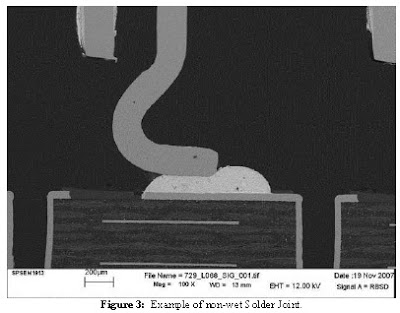
From the previous relationship, total wetting is achieved when the wetting angle equals 0° and total nonwetting is achieved when the wetting angle equals 180°. Thus, the closer the wetting angle approaches 0° the greater the wetting / solderability (Manko, 2001). IPC-A-610, a common industry standard for solder joint workmanship criteria and one of the most commonly used standards for many IBM products, states that for a solder joint to be acceptable the wetting angle has to be less then 90°. If the angle is greater then 90°, then the solder joint is considered a dewet or non-wet. There are some exceptions that are acceptable: when the wetting angle exceeding 90° is created by the solder contour extending over the edge of the solderable termination area or over solder resist. Figure 2 is an illustration that covers the acceptable wetting angles for solder joints. Figure 3 shows a classic non-wet solder joint.

During wetting, spreading has a greater speed then bulk material flow and thus, the amount of solder material present has little influence on the wetting angle. The greatest factors affecting the wetting angle are the following:

*Type of flux used
* How the flux is activated during reflow
* The solder metal alloy media
* Base metal material that is being soldered to
* Surface topography of the soldering surface
* Tarnish/oxidation layer thickness on the soldering surface
* Contaminants in the solder and solderable surface
* Rate of solidification of the solder on cooling (Manko, 2001).

will be contginued with experiments process...

domingo, 31 de octubre de 2010

INSPECTION TO IMPROVE LEAD-FREE SOLDER TECHNOLOGIES (Part 2)

Detection of Voids

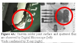
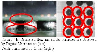
X-ray imaging in detection of voids is helpful to a certain extent. A Digital Microscope should be considered to work alongside, and not in place of or as alternative inspection equipment. Manufacturers striving to gain the highest quality should consider X-ray and Digital Microscope equipment as a pair. Detecting voids is a helpful example of this relationship.
During pre-heating, voids can occur due to deteriorated flux. This can result in low flowing solder causing gas pockets.
The surface of flux residue and shine of solder joints may indicate possible voids (Figure 4A and 4B).


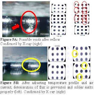
During reflow, air current that is too hot and strong deteriorates flux and causes voids (Figure 5A). The specialized BGA inspection lens for the Digital Microscope can work side by side with X-ray inspection, detecting possible voids. Adjusting air current can contribute to the reduction of void occurrence (Figure 5B). X-ray is an important aid for void detection and until now has been considered an alternative and separate solution apart from both stereo and digital microscopy. Inspection of BGA properties and defects should be considered from a combination of potential solution providers.

Judgment of Defects by Exterior Inspection
BGA exterior inspection allows access to the hardest to reach places on the PCB. The highly accessible prism adapter for the Digital Microscope BGA Lens can squeeze between components and look directly at the BGA from the side on heavily populated boards with minute pitches. Utilizing a metal halide bulb (discussed below), will greatly enhance the information retrieved from this style of observation. The following section as well will provide further examples of how specific reflections further support conclusions and information gathering. Without even the aid of X-ray technology it is possible to determine defects caused by over extended pre-heating and reflow (Figure 6).


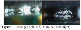
Common among these issues of over-heating are oxidization and visible damage to the ball itself (Figure 7). Exterior inspection goes beyond defects, aiding as well in the correction of

temperature profiles.


martes, 19 de octubre de 2010

Inspection to Improve Lead-Free Solder (Part 1)

INSPECTION TO IMPROVE LEAD-FREE SOLDER TECHNOLOGIES


Kazuo Kawai
Hirox-USA and Seika Machinery, Inc.
River Edge, NJ, USA and Torrance, CA, USA
info@hirox-usa.com and info@seikausa.com


ABSTRACT

Lead-free solders are said to cause various problems such as lack of self-alignment, bridges, solder balls, insufficient wetting, dendrites, pits, voids and peeling of soldering land. Also, on miniaturized lands, there may occur insufficient melting of solder paste. Even though these problems have not yet been resolved, lead-free soldering technologies have already been introduced at mass production sites. Most of these problems basically arise from heightened packaging temperature requirements in line with higher melting points of soldering materials.

Inspection of manufactured products to determine quality of the temperature profile and proper solder connection needs to be done with a high performance inspection system.

This technical paper and presentation will go over defects that can be uncovered by a high performance inspection system and merits of capturing images of such defects early during the assembly process. Without detection there may be a risk of damaging PCBs or parts that require rework. As well, serious quality problems or failures in the market after production may occur. The longer the lag time in detection of the defects, the higher the percentage of PCBs that may be scrapped. Therefore, inspection should take place at the earliest possible stage. Current technology available with a high end digital microscope will allow for immediate and thorough discovery of these defects which is of vital importance for SMT assembly.

Since lead-free solders were introduced to PCB assemblies, many soldering issues have arisen and for many, remain unsolved. This case study introduces the advantages of utilizing the digital microscope to identify soldering defects and root causes to improve productivity of lead-free soldering.
Although leaded and lead-free solders are different in their melting point, the basic theory in the SMT process, including temperature profiles, is still the same. However, the spreading property of lead-free solder is inferior to leaded solders. Therefore, determining good lead-free solder joints requires more detailed inspections than lead ones.
The appearance of flux residue helps to provide enough information for the temperature conditions of the solder joints being inspected. If wrong temperature conditions are used during the soldering process, there is a good chance ofvoids and insufficient spreading of solder. Observation of flux residue in addition to light reflection and shape of solder fillets are essential in the inspection of lead-free solder joints.
The following will provide the reader with many examples and various uses of a Digital Microscope as an exterior inspection as well as defect analysis tool for SMT. It is important as well to consider in the following pages, a comparison between Stereo Microscopy, lighting techniques, and use of adapters to aid inspection.
Key words: Digital Microscope, 360° Rotational Adapter, BGA Inspection Lens

LEAD-FREE SOLDER AND DIGITAL MICROSCOPY
Exterior Observation Using a Digital Microscope System
Excluding temperature profile graphs and X-ray imaging, all of the following images provided for visual aid of PCB components and BGA’s were captured with a Digital Microscope. The multiple oblique angles shown in the images are made possible by a 360° rotational adapter attached to the end of the Digital Microscope Lens itself. A specialized BGA lens allows for 90° inspection of BGA’s by means of a thin, flexible, plastic prim chip adapter. The benefit of using the 360° rotational adapter over stereo microscopy is in the rotation. Varying the angle of inspection on lead-free solder enhances assessment of solder shape and provides changes in reflection to help determine temperature profiles. This technique is not possible on lenses other than a Digital Microscope without configuring the lens, stage, and sample to fit the desired angle. In addition, by using a specialized BGA inspection lens, the same process described above can be applied when determining BGA shape and temperature profile. This simple yet beneficial approach to exterior observation can improve product quality on the production line. The addition of a Digital Microscope as a part of production rather than post- production Quality Control or Failure Analysis can support and expand the foundation of a company’s philosophy of quality and drive down costs on the product assembly line. The following nine sections will discuss the usefulness of a Digital Microscope as a part of PCB production and the potential effect its use can impart to product quality.

BRINGING THE DIGITAL MICROSCOPE TO THE PRODUCTION FLOOR

Any inspection done in-line during product assembly has to be quick, easy, and accurate in order to be seamlessly inserted into a company’s current standards for production. A Digital Microscope can cover both of these necessities while providing high quality images wherein observations and judgments can be made in seconds, observing defects before they reach Quality Control or Failure Analysis Divisions. This can potentially save time and money by integrating aspects of QC/FA into the production line, as well as help Process Engineering Teams attain solutions to problems more quickly.
The first portion to follow begins with examples concerning flux residue, and the ability of the 360° rotational adapter to gain information that up until now could not be easily gathered and stored by a stereo microscope. The sections following that will further support the use of a Digital Microscope, its rotational adapter, and the BGA inspection lens directly on the production line.

Judgment of Thermal Balance with Inspection of Flux Residue
Note: To see flux residue easily, leads were intentionally shifted from the lands (Figure 1A, 1B).
Access to these views have not been obtained by shifting or angling the PCB in any way, but were identified and captured using the 360° rotational adapter without having to manipulate the PCB in any way. Such rotation can easily show the flux residue as in these examples: showing flux spattering, Figure 1A (before pre-heat fan speed change), normal flux residue, Figure 1B (after pre-heat fan speed slow down), normal flux residue condition, Figure 2A and flux bridging, Figure 2B.


Solder melts and flows in accordance with the flux only reaching areas that the flux exists. Flux moves from the resist to the heated land by its tension, and if kept from deteriorating in pre-heating, lead-free solder will be more likely to self-align to the heated land by its surface tension (Figure 3).

martes, 16 de febrero de 2010

BGA - REWORK PROCESS. (Part 1)

Many PCB manufacturers have mistakenly delayed the incorporation of Ball Grid Array (BGA) packages into their product designs because of concerns over increased cost and complexity. Incorporating BGAs will not only require additional expenditures in equipment, but will also require additional skills training for employees. The increasing I/O capacity of BGAs and the need to provide more sophistication in less space, has forced many manufacturers to convert to BGA practices or risk losing their competitive advantage. As with any other component package, BGA rework capability is a necessary reality, and must be considered. Some important considerations for successfully reworking BGAs will be examined.

Removal Equipment

In selecting BGA rework equipment, some key elements are essential in obtaining versatility, reliability, and repeatability. Equipment available for BGA rework should incorporate the use of a split-vision alignment system to ensure the exact alignment of the component to the substrate. There should also be a programmable localizer reflow system, preferably one that uses hot-air convection while providing underside heating to ensure the correct reflow of the BGA. Some typical examples are the standard "hot gas" method, the sealed oven method, the horizontal flow method, and the conduction method. Also required will be an assortment of tools including a solder wick, a soldering iron with a wide chisel tip, and a micro-stencil for the application of solder paste if necessary. Finally, one very important factor in successful rework of any BGA begins in the design stage of the assembly. Ensuring enough free area (“keep-out distance”) around the periphery of the BGA is important to provide enough clearance for rework tooling and fixturing. In most cases, a "keep out distance" of 0.100in. is sufficient.